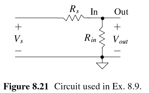
Let’s begin by adding the noise voltage spectral density to the circuit, Fig. 8.22a. The output noise PSD is
V o n o i s e 2 ( f ) = 4 k T R s [ R i n R i n + R s ] 2 + 4 k T R i n [ R s R i n + R s ] 2 V_{o n o i s e}^{2}(f)=4k T R_{s}\biggl[\frac{R_{i n}}{R_{i n}+R_{s}}\biggr]^{2}+4k T R_{i n}\biggl[\frac{R_{s}}{R_{i n}+R_{s}}\biggr]^{2} V o n o i s e 2 ( f ) = 4 k T R s [ R i n + R s R i n ] 2 + 4 k T R i n [ R i n + R s R s ] 2
To determine V o n o i s e , R M S V_{o n o i s e,R M S} V o n o i s e , R M S , we integrate this PSD over the bandwidth of interest B or
V o n o i s e , R M S 2 = ∫ f L f H V o n o i s e 2 ( f ) ⋅ d f = 4 k T B R s [ R i n R i n + R s ] 2 + 4 k T B R i n [ R s R i n + R s ] 2 V_{o n o i s e,R M S}^{2}=\int_{f_{L}}^{f_{H}}V_{o n o i s e}^{2}(f)\cdot d f=4k T B R_{s}\biggl[{\frac{R_{i n}}{R_{i n}+R_{s}}}\biggr]^{2}+4k T B R_{i n}\biggl[{\frac{R_{s}}{R_{i n}+R_{s}}}\biggr]^{2} V o n o i s e , R M S 2 = ∫ f L f H V o n o i s e 2 ( f ) ⋅ d f = 4 k T B R s [ R i n + R s R i n ] 2 + 4 k T B R i n [ R i n + R s R s ] 2
Noting our gain A (= V o u t / V i n V_{_{o u t}}/V_{i n} V o u t / V i n not V o u t / V s V_{_{o u t}}/V_{s} V o u t / V s ) is one, we can use the model shown in Fig. 8.22b. To determine the input-referred noise sources, we can use Eq. (8.32) and the results in Ex. 8.7 . To determine V i n o i s e , R M S \textstyle V_{i n o i s e,R M S} V i n o i s e , R M S , we short the input to ground (R s = 0 R_{s}=0 R s = 0 in Fig. 8.21 and the equation above), Fig. 8.22c, and equate the circuit output to V o n o i s e , R M S \textstyle V_{o n o i s e,R M S} V o n o i s e , R M S . This gives
V o n o i s e , R M S 2 = 4 k T R s B ⋅ ( A R i n R s + R i n ) 2 + I i n o i s e , R M S 2 ⋅ ( A R s R i n R s + R i n ) 2 + V i n o i s e , R M S 2 ⋅ ( A R i n R s + R i n ) 2 V_{o n o i s e,R M S}^{2}=4k T R_{s}B\cdot\left(\frac{A R_{i n}}{R_{s}+R_{i n}}\right)^{2}+I_{i n o i s e,R M S}^{2}\cdot\left(\frac{A R_{s}R_{i n}}{R_{s}+R_{i n}}\right)^{2}+V_{i n o i s e,R M S}^{2}\cdot\left(\frac{A R_{i n}}{R_{s}+R_{i n}}\right)^{2} V o n o i s e , R M S 2 = 4 k T R s B ⋅ ( R s + R i n A R i n ) 2 + I i n o i s e , R M S 2 ⋅ ( R s + R i n A R s R i n ) 2 + V i n o i s e , R M S 2 ⋅ ( R s + R i n A R i n ) 2 (8.32)
V o n o i s e , R M S , R s = 0 = V i n o i s e , R M S = 0 V_{o n o i s e,R M S,Rs=0}=V_{i n o i s e,R M S}=0 V o n o i s e , R M S , R s = 0 = V i n o i s e , R M S = 0
To determine I i n o i s e , R M S \textstyle I_{i n o i s e,R M S} I i n o i s e , R M S , we open the input (R s = ∞ R_{s}=∞ R s = ∞ ), Fig. 8.22d, and equate the Rs circuit’s output to V o n o i s e , R M S \textstyle V_{o n o i s e,R M S} V o n o i s e , R M S (from the equation above). This gives
R i n 2 ⋅ I i n o i s e , R M S 2 = V o n o i s e , R M S , R s = ∞ 2 = 4 k T B R i n → I i n o i s e , R M S = 4 k T B R i n R_{i n}^{2}\cdot I_{i n o i s e,R M S}^{2}=V_{o n o i s e,R M S,R s=\infin }^{2}=4k T B R_{i n}\to I_{i n o i s e,R M S}=\sqrt{\frac{4k T B}{R_{i n}}} R i n 2 ⋅ I i n o i s e , R M S 2 = V o n o i s e , R M S , R s = ∞ 2 = 4 k T B R i n → I i n o i s e , R M S = R i n 4 k T B
The input SNR is given in Eq. (8.29). The output SNR, Fig. 8.22e, is
S N R i n = V s , R M S 2 ⋅ [ R i n R i n + R s ] 2 4 k T R s B ⋅ [ R i n R i n + R s ] 2 = V s , R M S 2 4 k T R s B S N R_{i n}=\frac{V_{s,R M S}^{2}\cdot\left[\frac{R_{i n}}{R_{i n}+R_{s}}\right]^{2}}{4k T R_{s}B\cdot\left[\frac{R_{i n}}{R_{i n}+R_{s}}\right]^{2}}=\frac{V_{s,R M S}^{2}}{4k T R_{s}B} S N R i n = 4 k T R s B ⋅ [ R i n + R s R i n ] 2 V s , R M S 2 ⋅ [ R i n + R s R i n ] 2 = 4 k T R s B V s , R M S 2 (8.29)
S N R o u t = V s , R M S 2 ⋅ [ R i n R s + R i n ] 2 V o n o i s e , R M S 2 = V s , R M S 2 4 k T B ⋅ R s ( 1 + R s / R i n ) \mathrm{SN}R_{o u t}={\frac{V_{s,R M S}^{2}\cdot\left[{\frac{R_{i n}}{R_{s^{+}R_{i n}}}}\right]^{2}}{V_{o n o i s e,R M S}^{2}}}={\frac{V_{s,R M S}^{2}}{4k T B\cdot R_{s}(1+R_{s}/R_{i n})}} S N R o u t = V o n o i s e , R M S 2 V s , R M S 2 ⋅ [ R s + R i n R i n ] 2 = 4 k T B ⋅ R s ( 1 + R s / R i n ) V s , R M S 2 (8.40)
The noise factor is then
F = 1 + R s R i n F=1+\frac{R_{s}}{R_{i n}} F = 1 + R i n R s (8.41)
To minimize the NF, we can decrease R s R_{s} R s or increase R i n R_{in} R i n . Decreasing R s R_{s} R s causes S N R i n SNR_{in} S N R i n and S N R o u t SNR_{out} S N R o u t to increase, as seen in Eqs. (8.29) and (8.40). At the same time, increasing R i n R_{in} R i n causes S N R o u t SNR_{out} S N R o u t to move towards S N R i n SNR_{in} S N R i n , Eq. (8.40), resulting in F moving towards 1.