Question 30.2: Suppose that the 2R MSB resistor in the DAC described in Ex.......
Suppose that the 2R MSB resistor in the DAC described in Ex. 30.1 experiences a 0.5% mismatch. Estimate the resulting DAC’s INL and DNL. Use SPICE to verify your answer.
Learn more on how do we answer questions.
The 0.5% mismatch (ΔR/R or 1 σ [standard deviation]) is the mismatch specified for the unsilicided n+ polysilicon resistors in Table 4.1. Again it is desirable to use poly resistors because they sit above the substrate, on the field oxide, and are more immune to substrate noise. Note that the voltage coefficient can (will) also cause nonlinearities. However, instead of the worst-case situation of an abrupt mismatch between the lower resistors and the MSB 2R resistor, as used in this example, a first-order voltage coefficient error will cause a linear variation of the resistor values from the LSB resistor up to the MSB resistor and so the effects of the voltage coefficient, for reasonably small values, are generally not significant compared to the random mismatch effects.
Rewriting Eqs. (30.14) and (30.15) to estimate the maximum number of bits possible with 1 LSB INL or DNL results in
\mathrm{Resistor~mismatch}=\left|\frac{\Delta R}{R}\right|\leq\frac{1}{2^{N-1}} (30.14)
\Delta{I}=\frac{V_{R E F+}-V_{R E F-}}{2(R+\Delta R)}-\frac{V_{R E F+}-V_{R E F-}}{2R}\approx-\frac{V_{R E F+}-V_{R E F-}}{2}\cdot\frac{\Delta R}{{(R+\Delta R)\cdot R}} (30.15)
N=1-3.3\cdot\log\left\lgroup\frac{\Delta R}{R}\right\rgroup (30.20)
Using this equation with ΔR/R = 0.005 results, again, in N = 8.6 bits. For a 10-bit DAC, we would estimate both the INL and DNL as 2.4 bits.
To verify these results using SPICE, let’s input a code of 01 1111 1111 (ideally 499 mV) and then step the input code to 10 0000 0000 (ideally, 500 mV).
With the MSB 2R resistor changed to 20.1k (a 0.5% mismatch from its ideal 20k value) the simulation results are shown in Fig. 30.16. With this mismatch the output of the DAC is 500.3 mV when the input is 01 1111 1111. The INL with this input code is 1.25 LSBs (roughly 1.5 mV). The INL when the input digital code is 10 0000 0000 is -1.25 LSBs. The DNL at this worst-case point is -2.5 LSBs. Note that the DAC is nonmonotonic (DNL < -1 LSB). An increase in the digital input code results in a decrease in the output voltage. Nonmonotonic DACs can result in circuits that don’t function properly (an example being a successive approximation ADC). A DNL of -1 LSB would indicate the output voltage of the DAC doesn’t change when the input code changes.
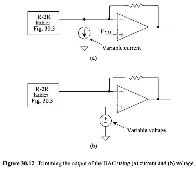
To improve the DNL, the upper bits of the DAC must be segmented as seen in Fig. 30.6. Improving the INL relies on calibrating out the mismatch errors (see Figs. 30.12 and 30.13). Also note, again, that mismatch can be improved by layout techniques (e.g., common centroid) and by averaging the outputs of multiple resistor strings.
Table 4.1 Typical properties of resistive materials in a nm CMOS process.
| Sili-cide | Resistor type | R_{square} (ohms/sq) AVG. | TCR1 (ppm/C) AVG. | TCR2 (ppm/C²) AVG. | VCR1 (ppm/V) AVG. | VCR2 (ppm/V² ) AVG. | Mis-match % \Delta R/R |
| N/A | well | 500 ± 10 | 2400 ± 50 | 7 ± 0.5 | 8000 ± 200 | 500 ± 50 | < 0.1 |
| No | n+ poly | 200 ±1 | 20 ± 10 | 0.6 ± 0.03 | 700 ± 50 | 150 ± 15 | < 0.5 |
| No | p+ poly | 400 ± 5 | 160 ± 10 | 0.8 ± 0.03 | 600 ± 50 | 150 ± 15 | < 0.2 |
| No | n+ | 100 ± 2 | 1500 ± 10 | 0.04 ± 0.1 | 2500 ± 50 | 350 ± 20 | < 0.4 |
| No | P+ | 125 ± 3 | 1400 ± 20 | 0.4 ± 0.1 | 80 ± 80 | 100 ± 25 | < 0.6 |
| Yes | n+ poly | 5 ± 0.3 | 3300 ± 90 | 1.0 ± 0.2 | 2500 ± 125 | 3800 ± 400 | < 0.4 |
| Yes | p+ poly | 7 ± 0.1 | 3600 ± 50 | 1.0 ± 0.2 | 2500 ± 400 | 5500 ± 250 | < 0.7 |
| Yes | n+ | 10 ± 0.1 | 3700 ± 50 | 1.0 ± 0.2 | 350 ± 150 | 600 ± 60 | < 1.0 |
| Yes | P+ | 20 ± 0.1 | 3800 ± 40 | 1.0 ± 0.2 | 150 ± 50 | 800 ± 40 | < 1.0 |