Question 30.8: Simulate the operation of the S/Hs shown in both Figs. 30.31......
Simulate the operation of the S/Hs shown in both Figs. 30.31 and 30.34. Assume the S/H is clocked at 100 MHz, \nu _{in+} is a sinewave that swings from ground to VDD, and \nu _{in-} is connected to V_{CM}(the input signal is single-ended and covers the entire supply range). Show how the op-amp’s input common-mode voltage range changes or doesn’t change. Assume all capacitors are 1 pF and then show how a 10% mismatch in the capacitors affects the output of the S/H.


Learn more on how do we answer questions.
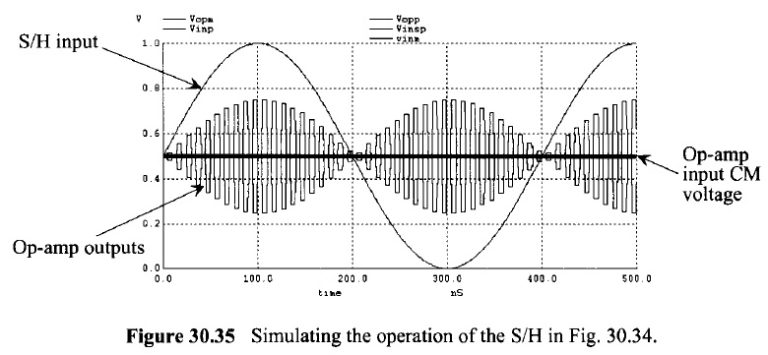
Figure 30.35 shows the simulation results for the S/H seen in Fig. 30.34. Notice how the op-amp’s input common-mode voltage stays constant at V_{CM}. While the simulation results show the op-amp’s outputs, \nu _{o+} and \nu _{o-} , and not the difference in the outputs, if we do take the difference (with all capacitors at 1 pF and so the gain of the S/H should be one) we indeed see that the gain is one. Next if we modify the simulation and change one C_I capacitor to 1.1 pF the simulation results show a gain error. As we’ll discuss in a moment the big benefit of using the topology seen in Fig. 30.31 is that capacitor matching isn’t important.
Next, Fig. 30.36 shows the simulation results for the S/H seen in Fig. 30.31. In part (a) the input common-mode voltage of the op-amp is shown. When the \phi_1 switches are closed, the voltage returns to V_{CM} (the op-amp is placed in a follower configuration where the input signal charges the two capacitors). The input common mode voltage varies between 750 mV and 250 mV, a concern for most op-amp designs using a single input diff-amp. In part (b) the rail-to-rail input signal is converted into a differential S/H output signal. Note that the gain of the S/H is one. Note also how, unlike the op-amp outputs in Fig. 30.33, the outputs are limited to V_{CM} + V_P/2 where V_p is the peak amplitude of the input sinewave (= 500 mV here). When the input sinewave has an amplitude of 1 V (500 mV above V_{CM}), the positive output is 750 mV and the negative op-amp output is 250 mV.
Subtracting the op-amp outputs results in 500 mV (the same voltage as the input signal referenced to V_{CM}). It’s important to understand how going from a single-ended signal to a fully-differential signal may result in a reduction in the op-amp output swing.
The simulation results seen in Fig. 30.36 were generated using 0.9 pF and 1.0 pF sampling capacitors (labeled C_F in Fig. 30.31). Because the feedback factor is unity, these capacitors will not affect the gain of the S/H. The point here is that the matching of the capacitors isn’t important for a precise gain of one when using this (Fig. 30.31) S/H topology. (The op-amp open-loop gain, however, is still important.) Again, while the topology seen in Fig. 30.34 is sensitive to capacitor matching, it still may be the S/H topology of choice because the op-amp’s input CMR remains constant with a single-ended input signal.