Question 12.10: Objective: Design a feedback amplifier to provide a given cu...
Objective: Design a feedback amplifier to provide a given current gain. Specifications: Assume that a signal current source has a nominal output resistance of R_{S} = 10 kΩ and that the amplifier will drive a nominal load of R_{L} = 50 Ω. A current gain of 10 is required.
Choices: An op-amp with the same characteristics described in Example 12.8 is available.
Learn more on how we answer questions.
(Design Approach): An amplifier with a low input resistance and a large output resistance is required, to minimize loading effects at the input and output. For these reasons, a shunt–series feedback configuration, or current amplifier, will be used.
The closed-loop gain is
A_{if} = 10 \cong 1/β_{i}
and the feedback transfer function is β_{i} = 0.1.
The dependent open-loop voltage source of the op-amp, as shown in Figure 12.17, can be transformed to an equivalent dependent open-loop current source, as shown in Figure 12.9. We find that
A_{i} = A_{v} R_{i}/R_{o}
Using the parameters specified for the op-amp, we find A_{i}= 10^{6} . The loop gain for the shunt–series configuration is
A_{i} β_{i} = (10^{6}))(0.1) = 10^{5}
Referring to Table 12.1, we expect the input resistance to be
| Table 12.1 | Summary results of feedback amplifier functions for the ideal feedback circuit | ||||
| Feedback amplifier | Source signal | Output signal | Transfer function | Input resistance | Output resistance |
| Series–shunt (voltage amplifier) | Voltage | Voltage | A_{vf} = \frac{V_{o}}{V_{i}} = \frac{A_{v}}{(1 + β_{v} A_{v})} | R_{i}(1 + β_{v} A_{v}) | \frac{R_{o}}{(1 + β_{v} A_{v})} |
| Shunt–series (current amplifier) | Current | Current | A_{if} = \frac{I_{o}}{I_{i}} = \frac{A_{i}}{(1 + β_{i} A_{i})} | \frac{R_{i}}{(1 + β_{i} A_{i})} | R_{o}(1 + β_{i} A_{i}) |
| Series–series (transconductance amplifier) | Voltage | Current | A_{gf} = \frac{I_{o}}{V_{i}} = \frac{A_{g}}{(1 + β_{z} A_{g})} | R_{i}(1 + β_{z} A_{g}) | R_{o}(1 + β_{z} A_{g}) |
| Shunt–shunt (transresistance amplifier) | Current | Voltage | A_{zf} = \frac{V_{o}}{I_{i}} = \frac{A_{z}}{(1 + β_{g} A_{z})} | \frac{R_{i}}{(1 + β_{g} A_{z})} | \frac{R_{o}}{(1 + β_{g} A_{z})} |
R_{i f} = 10/10^{5} k \Omega → 0.1 \Omega
and the output resistance to be
R_{of} = (100)(10^{5}) \Omega → 10 M \Omega
These resistance values will minimize any loading effects at the amplifier input and output.
For the shunt–series configuration in Figure 12.20, we have
\frac{1}{β_{i}} = 1 + \frac{R_{F}}{R_{1}} = 10
or
R_{F}/R_{1} = 9
For our purposes, R_{1} must be fairly small, to avoid a loading effect at the output.
However, R_{1} must not be too small, to avoid large currents in the amplifier. Therefore, we choose R_{1} = 1 k\Omega and R_{F} = 9 k\Omega.
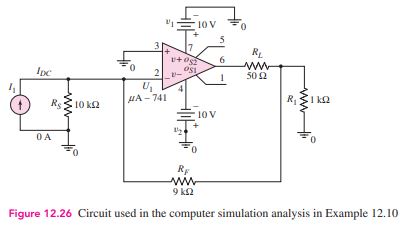
Computer Simulation Verification: Figure 12.26 shows the circuit used in the computer simulation. A standard µA-741 op-amp was used in the circuit. The current gain was found to be exactly 10.0. The input resistance R_{i f} looking into the op-amp with feedback was found to be 0.056 Ω, which compares favorably to the predicted value of 0.1 Ω. The output resistance seen by the load resistor was found to be approximately 200 MΩ. This value is on the order of 20 times larger than the predicted value, but is closer to the ideal value. The differences between predicted and measured values are due to the differences in assumed op-amp parameters and the µA-741 op-amp parameters.
Comment: This design also produces an almost ideal feedback current amplifier, if reasonable values of feedback resistors are used