Question 8.17: Estimate the input-referred noise for the circuit seen in Fi......
Estimate the input-referred noise for the circuit seen in Fig. 8.34.

Learn more on how do we answer questions.
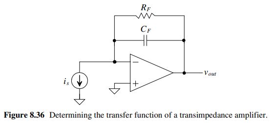
This amplifier is a transimpedance amplifier, that is, current input and voltage output. The amplifier takes the current generated by the photodiode and converts it into an output voltage. The low-frequency gain of the amplifier is RF or 100k.
The 1,000 pF feedback capacitor limits the bandwidth of the circuit to reduce noise. The photodiode is reverse-biased. Its noise contributions are related to the conversion of light to electrons (which we won’t add to our noise analysis). The diode’s reverse leakage current will be small and so the shot noise contributions to the circuit noise will be insignificant. The op-amp holds the diode’s anode at a fixed potential (ground). The diode’s junction capacitance won’t affect the noise in the circuit (both sides of the capacitance are at AC ground).
The basic noise circuit for Fig. 8.34 is seen in Fig. 8.35. All of the output is fed back to the input so that the op-amp’s thermal and flicker noise sources appear directly in the output signal (to keep the inverting and noninverting terminals at the same potential). The resistor’s thermal noise (keeping in mind that we only look at one noise source at a time so that the inverting and noninverting inputs of the op-amp are at 0V), will create an output voltage that is the product of the noise current and the parallel combination of the 100k and 1,000 pF.
The output noise PSD can then be written as
Vonoise2(f)=f3.14×10−15+64×10−18+RF4kT⋅∣∣∣∣∣RF+1/jωCFRF⋅1/jωCF∣∣∣∣∣21+(2πf⋅RFCF)24kTRFWe should recognize the last term in this PSD as simply kT/C noise (Ex. 8.6). The bandwidth of the amplifier can be determined using Fig. 8.36 as
A(f)=Rm=isvout=RF∣∣jωCF1=1+jωRFCFRFIn other words the gain of the amplifier is RF(vout/iS) and its bandwidth is
f3dB=2πRFCF1which is 1.59 kHz. We can estimate the output RMS noise knowing the gain-bandwidth product, fun, of the TLC220 op-amp is 2 MHz, the gain of the op-amp’s input-referred noise to the output is one (and thus has a bandwidth of 2 MHz), and using Eqs. (8.56), (8.15), and (8.24) as
Vnoise,RMS=7⋅FNN Volts (8.56)
Vonoise,RMS2=VLF,noise2⋅f3dB⋅[tan−1f/f3dB]0∞=VLF,noise2⋅ f3dB⋅2πNEB (8.15)
Vonoise,RMS=2πRC1⋅2π⋅4kTR=CkT (8.24)
Vonoise,RMS2=49⋅3.14×10−15=154×10−15+64×10−18⋅2π⋅2MHz=200×10−12+CFkT=4×10⁻¹²Vonoise,RMS≈(0.392)2+(14.14)2+(2.07)2=14.3μV
The op-amp’s thermal noise dominates the output RMS noise. Our estimate for the flicker noise is high. However, it’s easy to throw some numbers in for high and low frequencies in Eq. (8.55) and convince ourselves that the result isn’t impacted too much. For example, we used ln10−101011≈49 (yes, it’s closer to 48 but we use 49 ln 1011 10 10 49 because the square-root is a whole number, i.e., 7) when we derived Eq. (8.55). If we were to use instead ln10−10105 (a million times smaller upper frequency), we get 34.5 (a square root of roughly 6). The impact on the result is too small to worry about (unless, of course, the bandwidth is very narrow as in Ex. 8.16).
Vnoise,RMS2=fL∫fHfFNN⋅df=FNN⋅lnfLfH units of V² (8.55)
Dropping the feedback capacitance to 1 pF increases the bandwidth to 1.59 MHz and increases the RMS output noise due to RF (kT/C noise) to 64 μV.
Our output signal is determined using is⋅RF. An SNRout of 0 dB, in this example with CF=1,000 pF, would correspond to an is of roughly 143 pA (=Iinoise,RMS=Vonoise,RMS/RF). If we wanted an input signal to produce an output that is larger than the peak-to-peak value of the output noise (here, from Fig. 8.33, > 6 × 14.3 μV), then is>858pA.