Question 3.13: For the BJT circuit in Fig. 3.43, β = 150 and VBE = 0.7 V. F...
For the BJT circuit in Fig. 3.43, β = 150 and V_{B E}=0.7 V . \text { Find } v_{o} .

Learn more on how we answer questions.
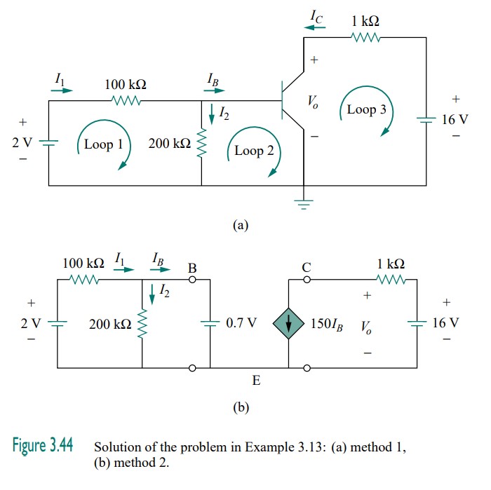
We can solve this problem in two ways. One way is by direct analysis of the circuit in Fig. 3.43. Another way is by replacing the transistor with its equivalent circuit.
METHOD 1 We can solve the problem as we solved the problem in the previous example. We apply KVL to the input and output loops as shown in Fig. 3.44(a). For loop 1,
2=100 \times 10^{3} I_{1}+200 \times 10^{3} I_{2} (3.13.1)
For loop 2,
V_{B E}=0.7=200 \times 10^{3} I_{2} \quad \Longrightarrow \quad I_{2}=3.5 \mu A (3.13.2)
For loop 3,
-v_{o}-1000 I_{C}+16=0
or
v_{o}=16-1000 I_{C} (3.13.3)
From Eqs. (3.13.1) and (3.13.2),
\begin{gathered}I_{1}=\frac{2-0.7}{100 \times 10^{3}}=13 \mu A , \quad I_{B}=I_{1}-I_{2}=9.5 \mu A \\I_{C}=\beta I_{B}=150 \times 9.5 \mu A =1.425 mA\end{gathered}
Substituting for I_{C} in Eq. (3.13.3),
v_{o}=16-1.425=14.575 V
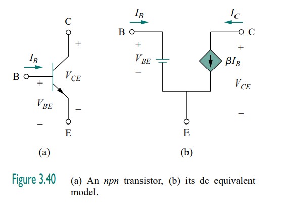
METHOD 2 We can modify the circuit in Fig. 3.43 by replacing the transistor by its equivalent model in Fig. 3.40(b). The result is the circuit shown in Fig. 3.44(b). Notice that the locations of the base (B), emitter (E), and collector (C) remain the same in both the original circuit in Fig.3.43 and its equivalent circuit in Fig. 3.44(b). From the output loop,
v_{o}=16-1000\left(150 I_{B}\right)
But
I_{B}=I_{1}-I_{2}=\frac{2-0.7}{100 \times 10^{3}}-\frac{0.7}{200 \times 10^{3}}=(13-3.5) \mu A =9.5 \mu A
and so
v_{o}=16-1000\left(150 \times 9.5 \times 10^{-6}\right)=14.575 V