Question 4.11: A source degenerated cascode LNA as shown in Fig. 4.50(b) wi...
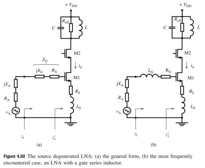
A source degenerated cascode LNA as shown in Fig. 4.50(b) will be designed for f_0 = 1.86 GHz (\omega_0 = 1.17\times 10^{10} rad/s). The restrictions are as follows.
The technology is similar to the AMS 0.35 micron technology but has a thick metal layer that permits us to realize reasonably high-Q on-chip inductors. The main parameters related to the NMOS transistors are C_{ox} = 4.54\times 10^{-7} F/cm^2, k_{ol}= 0.74,{}^{24} \mu_n = 325 (as an average value that corresponds to V_{GS} = 1 V^{25}). The numerical value of the A parameter is calculated as 2.47\times 10^{11}.
The DC current shall not exceed 4 mA.
The on-chip inductors will be chosen from a library that contains a number of wellcharacterized inductors: L = 0.5 nH, 1 nH, 2 nH, 5 nH and 10 nH and Q = 10 at 1.86 GHz.
The antenna is a “folded loop antenna” designed for 1.86 GHz, whose impedance is
Z_A = 44.7-j 9.73 ohm, for unbalanced use.{}^{26}
The temperature of the antenna and the average temperature of the chip are assumed to be 300 K and 330 K, respectively.
Learn more on how we answer questions.
The design can be initiated at one of several possible starting points. Let us start with (4.116), with a DC current smaller than the allowed maximum value to reserve a margin for probable iterations, and the possible minimum L_S value; I_D = 3 mA, L_S= 0.5 nH. It is necessary to estimate a value for R_A-(R_S + R_G) in (4.116), and check its validity later on. Let us assume R_A-(RS + RG) = 30 ohm. With these starting values (4.116) yields W = 508 μm that corresponds to C_{gs} = 597 fF according to (1.40). Now LG can be calculated from (4.118):
L_G=\frac{1}{(1.17\times 10^{10})^2(597\times 10^{-15})}-0.5\times 10^{-9}-(\frac{-9.73}{(1.17\times 10^{10})})=12.53 nHSince we have to use inductors from the library, it is necessary to perform an iteration with 10 nH, the closest inductor value to 12.53 nH. With L_G = 10 nH (4.118) yields C_{gs} = 755 fF, which corresponds to W = 642 μm. To satisfy (4.116) with this value and L_S = 0.5 nH, I_D must be 3.79 mA which is smaller than the allowed maximum value.
Now we must calculate the source and drain series resistance and check if the condition on (R_S + R_G) is reasonably close to the initial assumption.
R_S is the sum of the effective series resistance of LS and the inherent source series resistance of M1. The series resistance RSL of LS can be calculated from (4.14) as
R_{SL}=\frac{L_S \omega_0}{Q}=\frac{(0.5\times 10^{-9})(1.17\times 10^{10})}{10}\cong 0.585ohm
The inherent source series resistance of M1, R_{SM1} is calculated as in Example 4.10
and found to be 0.545 ohm. Therefore,
R_S=R_{SL}+R_{SM1}=1.13ohm
Similarly, the total series gate resistance, R_G, which is the sum of the effective series resistance of L_G and the inherent gate series resistance of M1 can be found as 12.52 ohm. With these values
R_A-(R_S+R_G)=44.7-(1.13+12.52)=31.05ohm
which is reasonably close to the initial assumption.
The parameters in (4.138) now can be calculated.
From (4.120)
\left|Y_{mG}(\omega_0)\right|^2=\frac{(44.7\times 10^{-3})^2}{\left[(44.7\times 10^{-3})\times 1.13\right]^2+ \left[2\times (1.17\times 10^{10})\times (755\times 10^{-15})\times 44.7\right]^2}=3.2\times 10^{-3}[S²]