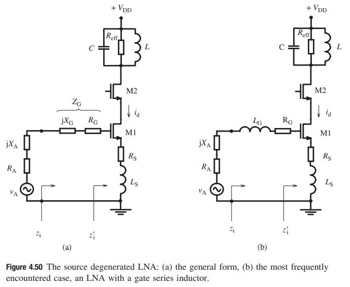
Question 4.11: A source degenerated cascode LNA as shown in Fig. 4.50(b) wi...
A source degenerated cascode LNA as shown in Fig. 4.50(b) will be designed for f_0 = 1.86 GHz (\omega_0 = 1.17\times 10^{10} rad/s). The restrictions are as follows.
The technology is similar to the AMS 0.35 micron technology but has a thick metal layer that permits us to realize reasonably high-Q on-chip inductors. The main parameters related to the NMOS transistors are C_{ox} = 4.54\times 10^{-7} F/cm^2, k_{ol}= 0.74,{}^{24} \mu_n = 325 (as an average value that corresponds to V_{GS} = 1 V^{25}). The numerical value of the A parameter is calculated as 2.47\times 10^{11}.
The DC current shall not exceed 4 mA.
The on-chip inductors will be chosen from a library that contains a number of wellcharacterized inductors: L = 0.5 nH, 1 nH, 2 nH, 5 nH and 10 nH and Q = 10 at 1.86 GHz.
The antenna is a “folded loop antenna” designed for 1.86 GHz, whose impedance is
Z_A = 44.7-j 9.73 ohm, for unbalanced use.{}^{26}
The temperature of the antenna and the average temperature of the chip are assumed to be 300 K and 330 K, respectively.
Our explanations are based on the best information we have, but they may not always be right or fit every situation.
Learn more on how we answer questions.