Question 3.4: Simulation and Estimation of Loop Settling Times A 3.7–4.3-G...
Simulation and Estimation of Loop Settling Times
A 3.7–4.3-GHz synthesizer with a step size of 1 MHz is required. A 40-MHz crystal oscillator, a charge pump with 2π · 100 μA output current and a VCO (operating from a 3V supply) are available. Design a fractional N synthesizer with a loop bandwidth of 150 kHz using these components. Estimate the settling time of the loop for a 30- MHz and 300-MHz frequency step. Simulate and compare.


Learn more on how we answer questions.
Solution: First, if the VCO is operating with a 3V supply and must have a 600-MHz tuning range, we can estimate that its K_{VCO} will be 200 MHz/V. In addition, since we know the charge pump current, we know that the K_{phase} will be 100 μA/rad. For a VCO with a nominal frequency of 4 GHz and a reference frequency of 40 MHz, the division ratio will be 100. The next step is to size the loop filter. A 3-dB frequency of 150 kHz requires a natural frequency of 75 kHz (see Example 3.2). Thus, components can be determined as
C_{1} =\frac{IK_{VCO} } {2\pi \cdot N\omega ^{2}_{n} } =\frac{2\pi \cdot 100 \mu A \cdot \left(2\pi \cdot 200\frac{MHz}{V} \right) }{2\pi \cdot 100\left(2\pi \cdot 75 KHz \right)^{2} } =5.66 nFIn order to set R, we need to pick a damping constant. Let us pick 1/√2, or 0.707, which is a popular choice. Now,
R=2\zeta \sqrt{\frac{2\pi \cdot N}{IK_{VCO} C_{1} } } =2\left(\frac{1}{\sqrt{2} } \right) \sqrt{\frac{2\pi \cdot 100} {2\pi \cdot 100 \mu A\left(2\pi \cdot 200\frac{MHz}{V} \right) \cdot 5.66 nF } } =530\Omegaand we will set C_{2} = 566 pF at one-tenth the value of C_{1} .
Now, a step in output frequency of 30 MHz and 300 MHz corresponds to a step in the reference frequency of 0.3 MHz and 3 MHz, respectively. We learned in Example 3.2 that the maximum input frequency step that can be tolerated for a system with these parameters is 1 MHz. Therefore, the first frequency step will be a linear one, and the output will follow the theory of the previous section.
Therefore, we expect that it will take approximately 15 μs to settle, as we discovered previously.
In contrast, the second frequency step will involve cycle slipping. For this nonlinear case, we use the formula given in (3.60) to estimate the acquisition time as
T_{s} =\frac{2C_{1} \Delta \omega N }{IK_{VCO} } =\frac{\Delta \omega }{\pi \omega ^{2}_{n} } (3.60)
T_{s} =\frac{\Delta \omega }{\pi \omega ^{2}_{n} } =\frac{2\pi \cdot 3 MHz} {\pi \left(2\pi \cdot 75 KHz\right)^{2} } =27\mu s
Therefore, complete settling in this case should take 27 μs, plus an additional 15 μs for phase lock.
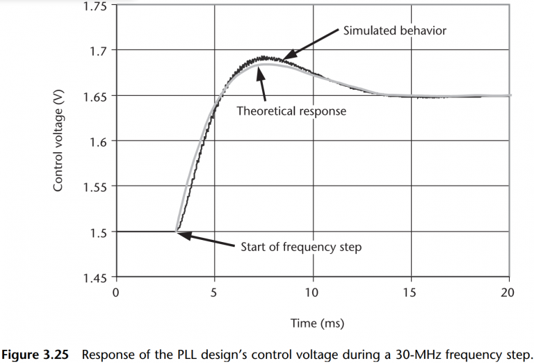
This behavior can be simulated using ideal components in a simulator such as Cadence’s Spectre. The blocks for the divider, VCO, PFD, and charge pump can be programmed using ideal behavioral models. These can be connected to the loop filter that has just been designed. From these simulations, we can look at the control voltage on the VCO to verify the performance of the loop. A plot of the response of the system to a 0.3-MHz step at its input, compared to simple theory, is shown in Figure 3.25. From this graph, it is easy to see that the simple theory does an excellent job of predicting the settling behavior of the loop with only a slight deviation. This small discrepancy is most likely due to the presence of C_{2} and to the sampling nature of the loop components.
The second frequency step can be simulated as well. The results of this simulation are plotted in Figure 3.26 and compared to the linear voltage ramp suggested by simple theory previously. In this case, this plot shows that the nonlinear response is predicted fairly well by the simple formula; however, the actual response is slightly faster. The tail of this graph is cut off, but the loop settled in about 39 μs, which is very close to the 42 μs predicted. The main difference between the simple estimate and reality is the fact that phase acquisition begins before the PLL actually reaches its final frequency value. We predicted it would begin in this simulation at 30 μs (when the simple theory predicts that the voltage ramp will reach its final value), but the linear portion of the graph actually starts earlier than this at about 25 or 26 μs. This accounts for our slightly pessimistic estimate. Still, such a simple estimate is remarkably good at predicting quite complicated behavior.