Question 8.6: STEPPED-IMPEDANCE FILTER DESIGN Design a stepped-impedance l...
STEPPED-IMPEDANCE FILTER DESIGN
Design a stepped-impedance low-pass filter having a maximally flat response and a cutoff frequency of 2.5 GHz. It is desired to have more than 20 dB insertion loss at 4 GHz. The filter impedance is 50 Ω; the highest practical line impedance is 120 Ω, and the lowest is 20 Ω. Consider the effect of losses when this filter is implemented with a microstrip substrate having d = 0.158 cm , \epsilon _{r}=4.2,\tan \pmb{\delta} =0.02 , and copper conductors of 0.5 mil thickness.
Learn more on how we answer questions.
To use Figure 8.26 we calculate
\frac{\pmb{\omega}}{\pmb{\omega}_{c}}-1=\frac{4.0}{2.5}-1=0.6;then the figure indicates N = 6 should give the required attenuation at 4.0 GHz.
Table 8.3 gives the low-pass prototype values as
TABLE 8.3 Element Values for Maximally Flat Low-Pass Filter Prototypes (g_{0} = 1, ω_c = 1, N = 1 to 10)
|
N |
g_{1} |
g_{2} |
g_{3} |
g_{4} |
g_{5} |
g_{6} |
g_{7} |
g_{8} |
g_{9} |
g_{10} |
g_{11} |
|
1 |
2.0000 |
1.0000 |
|||||||||
|
2 |
1.4142 |
1.4142 |
1.0000 |
||||||||
|
3 |
1.0000 |
2.0000 |
1.000 |
1.0000 |
|||||||
|
4 |
0.7654 |
1.8478 |
1.8478 |
0.7654 |
1.0000 |
||||||
|
5 |
0.6180 |
1.6180 |
2.0000 |
1.6810 |
0.6180 |
1.0000 |
|||||
|
6 |
0.5176 |
1.4142 |
1.9318 |
1.9318 |
1.4142 |
0.5176 |
1.0000 |
||||
|
7 |
0.4450 |
1.2470 |
1.8019 |
2.0000 |
1.8019 |
1.2470 |
0.4450 |
1.0000 |
|||
|
8 |
0.3902 |
1.1111 |
1.6629 |
1.9615 |
1.9615 |
1.6629 |
1.1111 |
0.3902 |
1.0000 |
||
|
9 |
0.3473 |
1.0000 |
1.5321 |
1.8794 |
2.0000 |
1.8794 |
1.5321 |
1.0000 |
0.3473 |
1.0000 |
|
|
10 |
0.3129 |
0.9080 |
1.4142 |
1.7820 |
1.9754 |
1.9754 |
1.7820 |
1.4142 |
0.9080 |
0.3129 |
1.0000 |
g_{1} = 0.517 = C_{1},
g_{2} = 1.414 = L_{2},
g_{3} = 1.932 = C_{3},
g_{4} = 1.932 = L_{4},
g_{5} = 1.414 = C_{5},
g_{6} = 0.517 = L_{6}.
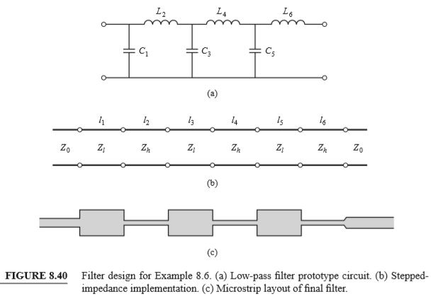
The low-pass prototype filter is shown in Figure 8.40a.
Next, (8.86a) and (8.86b) are used to replace the series inductors and shunt capacitors with sections of low-impedance and high-impedance lines. The required electrical line lengths, βℓ_i, along with the physical microstrip line widths, W_i, and lengths, ℓ_i, are given in the table below.
βℓ =\frac{LR_{0}}{Z_{h}} (inductor) (8.86a)
βℓ =\frac{CZ_{ℓ}}{R_{0}} (capacitor) (8.86b)
|
Section |
Z_{i}=Z_{ℓ} or Z_{h} (Ω) |
βℓ_{i} (deg) |
W_{i} (mm) |
ℓ_{i} (mm) |
|
1 |
20 |
11.8 |
11.3 |
2.05 |
|
2 |
120 |
33.8 |
0.428 |
6.63 |
|
3 |
20 |
44.3 |
11.3 |
7.69 |
|
4 |
120 |
46.1 |
0.428 |
9.04 |
|
5 |
20 |
32.4 |
11.3 |
5.63 |
|
6 |
120 |
12.3 |
0.428 |
2.41 |
The final filter circuit is shown in Figure 8.40b, with Z_{ℓ}=20 Ω and Z_{h}=120 Ω. Note that \beta ℓ<45^{\circ } for all but one section. The microstrip layout of the filter is shown in Figure 8.40c
Figure 8.41 shows the calculated amplitude response of the filter, with and without losses. The effect of loss is to increase the passband attenuation to about 1 dB at 2 GHz. The response of the corresponding lumped-element filter is also shown in Figure 8.41. The passband characteristic is similar to that of the stepped impedance filter, but the lumped-element filter gives more attenuation at higher frequencies. This is because the stepped-impedance filter elements depart significantly from the lumped-element values at higher frequencies. The stepped-impedance filter may have other passbands at higher frequencies, but the response will not be perfectly periodic because the lines are not commensurate.