Question 3.1: For the amplifier given in Fig. 3.8, the DC drain current (b...
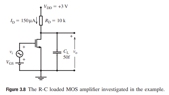
For the amplifier given in Fig. 3.8, the DC drain current (bias) of the transistor is I_D = 150 \mu A, therefore V_{DS} = 1.5 V. For this operating point the smallsignal parameters are g_m = 2 mS , C_{dg} = 20 fF, C_{gs} = 90 fF, and g_{ds} = 30 \mu S. The parasitic capacitance of the output node is assumed to be 10 fF.
Learn more on how we answer questions.
The low-frequency gain and the pole frequency can be calculated from (3.5) and (3.4b) as
s_0=+\frac{g_m}{C_{dg}}and s_p=-\frac{G_o}{C_o}=-\frac{(g_{ds}+G_L)}{(C_{op}+C_{dg}+C_L)} (3.4 b)
A_v(0)=-\frac{g_m}{G_o}=-\frac{g_m}{(G_L+g_{dg})} (3.5)
A_v(0)=-\frac{2\times 10^{-3}}{(3\times 10^{-6}\times 10^{-4})}=-15.38\Rightarrow 23.74 dB
f_p=\frac{1}{2\pi}\frac{(30\times 10^{-6}+10^{-4})}{2\pi (10\times 10^{-15}+20\times 10^{-15}+50\times 10^{-15})}=258.7 MHz
The input conductance for this frequency calculated from (3.11) is
g_{mi}(\omega_p)=\frac{g_{mi}(\omega\rightarrow \infty)}{2}=\frac{1}{2}\frac{C_{dg}}{C_o}(g_m+G_o\frac{C_{dg}}{C_o}) (3.11)
g_{mi}(f_p)=\frac{1}{2}\frac{20\times 10^{-15}}{80\times 10^{-15}}(2\times 10^{-3}+10^{-4}\frac{20\times 10^{-15}}{80\times 10^{-15}})=0.253\times 10^{-3}siemens
which corresponds to an input resistance of 3.95 kΩ! Even for one-tenth of the pole frequency, the input conductance is still high and can be calculated from (3.9a) as 4.95 μS,
g_{mi}(\omega)=\frac{C_{dg}}{C_o}(g_m+G_o\frac{C_{dg}}{C_o})\frac{1}{(\omega_p/\omega)+1} (3.9 a)
which corresponds to an input resistance of 200 kΩ.
This example proves that the input conductance of a common-source MOS amplifier has a frequency-dependent resistive component and this resistance can drop to considerably low values – which influences the output load of the previous stage or the signal source.
It is obvious that especially for high internal impedance signal sources, this frequency-dependent input conductance of the amplifier has to be taken into account.
Note that the input capacitance of the amplifier is the sum of C_{gs}, C_{dg} and C_{mi}.
In Fig. 3.7(b) the variation of the Miller capacitance is plotted as a function of ω.
It shows that the third component of the input capacitance has a value proportional to {g_m}/{G_o}
that is the magnitude of the Miller capacitance at low frequencies, and is usually high.
For the example given above, the value of the Miller capacitance is
C_{mi}(0)=C_{dg}\frac{g_m}{G_o}=20\times 10^{-15}\frac{2\times 10^{-3}}{130\times 10^{-6}}=307.7 fF
and the total input capacitance is
C_i=C_{gs}+C_{dg}+C_{mi}=90+20+307.7=417.7 fF
of which the dominant part is the Miller capacitance.
C_i capacitively loads the previous stage (or the driving signal source).
This high capacitive load affects the high-frequency performance of the previous stage and is the main reason for the deterioration of the high-frequency gain of multi-stage amplifiers.
In Fig. 3.9, the PSpice simulation results are shown for the amplifier given in Fig. 3.8.
The transistor is an AMS 0.6 μ NMOS device with L = 0.6 μm, W = 60 μm.
The drain current is 150 μA.
Small-signal parameters of this transistor are approximately equal to the values used in the example.
The frequency axes for the magnitude and phase characteristics (Fig. 3.9(a) and 3.9(b)) are intentionally drawn up to 30 GHz, to see the effects of the zero of the gain function.
The variations of the input admittance and the input capacitance, which is the sum of C_{gs}, C_{dg} and the C_{mi} Miller capacitance are given in Fig. 3.9(c) and (d).
The simulation results reasonably agree with the values calculated using the analytical expressions.

