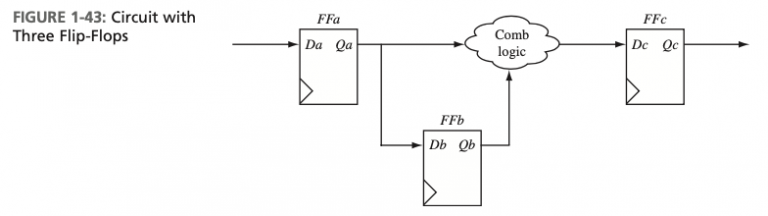
Question 1.2: Consider the circuit in Figure 1‐43 with the following minim...
Consider the circuit in Figure 1‐43 with the following minimum/maximum delays:
CLK‐to‐Q for flip‐flop A: 7ns/9ns
CLK‐to‐Q for flip‐flop B: 8ns/10ns
CLK‐to‐Q for flip‐flop C: 9ns/11ns
Combinational logic: 3ns/4ns
Setup time for flip‐flops: 2ns
Hold time for flip‐flops: 1ns
Compute the delays for all timing paths in this circuit and determine the maximum clock frequency allowed in this circuit.
Learn more on how we answer questions.
Remember that a timing path starts at either a primary input or at the input of a flip‐flop. A path terminates at the input of a flip‐flop or at a primary output.
Delay for path from flip‐flop A to B = t_{clk-to-Q(A)} + t_{su}(B) = 9ns +2ns =11ns
Delay for path from flip‐flop A to C = t_{clk-to-Q(A)} + t_{combo} + t_{su}(C) = 9ns +4ns +2ns =15ns
Delay for path from flip‐flop B to C = t_{clk-to-Q(B)} + t_{combo} + t_{su}(C) = 10ns +4ns +2ns =16ns
Delay for path from input to flip‐flop A = t_{su}(A) = 2ns =2ns
Delay for path from flip‐flop C to output = t_{clk-to-Q(C)}=11ns
Since the delay for path from B to C is the largest of the path delays, the maximum clock frequency is determined by this delay of 16ns. The frequency is 1/ t_{min} = 1/16ns=62.5MHz.