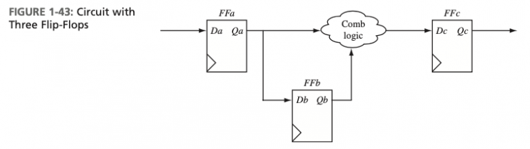
Question 1.2: Consider the circuit in Figure 1‐43 with the following minim...
Consider the circuit in Figure 1‐43 with the following minimum/maximum delays:
CLK‐to‐Q for flip‐flop A: 7ns/9ns
CLK‐to‐Q for flip‐flop B: 8ns/10ns
CLK‐to‐Q for flip‐flop C: 9ns/11ns
Combinational logic: 3ns/4ns
Setup time for flip‐flops: 2ns
Hold time for flip‐flops: 1ns
Compute the delays for all timing paths in this circuit and determine the maximum clock frequency allowed in this circuit.
The "Step-by-Step Explanation" refers to a detailed and sequential breakdown of the solution or reasoning behind the answer. This comprehensive explanation walks through each step of the answer, offering you clarity and understanding.
Our explanations are based on the best information we have, but they may not always be right or fit every situation.
Our explanations are based on the best information we have, but they may not always be right or fit every situation.
The blue check mark means that this solution has been answered and checked by an expert. This guarantees that the final answer is accurate.
Learn more on how we answer questions.
Learn more on how we answer questions.
Related Answered Questions
Question: 1.3
Verified Answer:
(a): Since XOR gate delay is higher than the AND g...
Question: 1.4
Verified Answer:
(a): This is a case of positive skew.
t_{cK...