Question 8.5: Design a single-ended ring oscillator operating at 1 GHz wit...
Design a single-ended ring oscillator operating at 1 GHz with phase noise of −100 dBc/Hz at a 1-MHz offset.
Learn more on how we answer questions.
In a 0.13-\mu m process, the power supply is typically 1.2V. We assume that the output voltage is 1V peak to peak, or 0.35 V_{rms} . Then, for three stages, phase noise can be predicted using (8.106),
PN(\Delta \omega) = \frac{8kT}{\nu ^{2}_{osc} } \frac{\sqrt{3} }{9\omega _{osc}C }(\frac{\omega _{osc} }{\Delta \omega } )^{2} (8.106)
\operatorname{PN}(\Delta \omega)=\frac{8 \times 4 \times 10^{-21} \times \sqrt{3} \times 2 \cdot \pi \cdot 1 \times 10^{9}}{0.35^{2} \times 9 \cdot C \cdot\left(2 \cdot \pi \cdot 1 \times 10^{6}\right)^{2}} = 1.27 × 10^{−33}\frac{\omega _{osc} }{C} = \frac{8.00×10^{-24} }{C }A phase noise of −100 dBc is 1 ×10^{-10}W. Solving for capacitance we find,
C = \frac{8.00×10^{-24} }{1×10^{-10} }= 8.00 × 10^{−14} = 80 fFThus, for a little bit of safety, we select a 100-fF capacitor, which results in a predicted phase noise of −101 dBc/Hz at a 1-MHz offset. This result will not be achieved unless special attention is paid to other details, like the minimization of 1/f noise. Otherwise, errors can be 10 dB or more, as this example will illustrate.
Using 100 fF, we can estimate the current it will take to achieve 1 GHz using (8.85),
f_{osc}= \frac{1}{T}= \frac{I}{NCV_{DD}} (8.85)
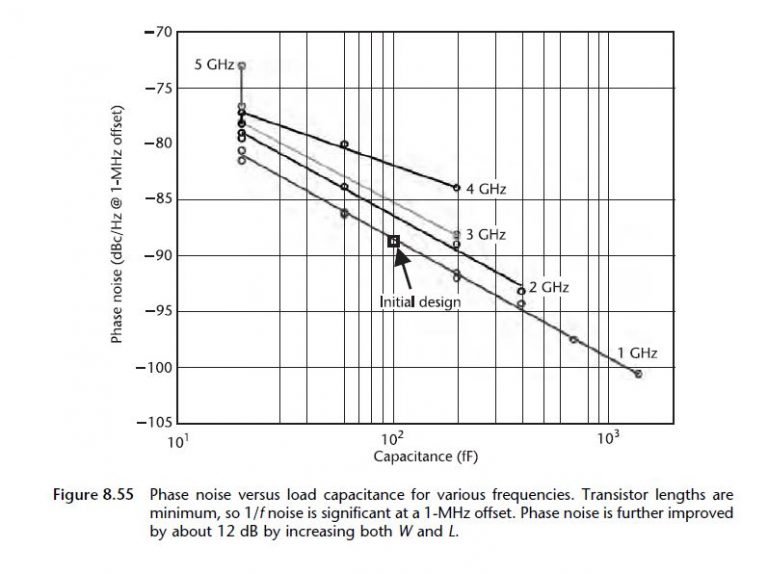
I = fNV_{DD} C = 1 × 10^{9} × 3 × 1.2 × 100 × 10^{−15} 360 \mu ATransistor sizing is done by considering current for maximum f_{T} . In this process, it is not practical to operate at maximum f_{T} since this requires a gate-to -source voltage of more than 1.2V. Instead, if the transistor size is increased by about five times, current density is down to about one-fifth of the current density for optimal f_{T} . More importantly, this results in the reduction of V_{GS} to about half of V_{DD} , but f_{T} is only reduced by about 20% of its maximum value, so this seems like a reasonable starting point. During the simulation iterations, using the circuit of Figure 8.46(a), the above current is adjusted to 330 \mu A with a total transistor width of 3 \mu m and minimum channel length. Simulation results show a phase noise of −88.7 dBc/Hz at a 1-MHz offset. Further exploration of phase noise versus capacitance, as shown in Figure 8.55, demonstrates that, as expected from (8.106), phase noise is inversely proportional to capacitance and proportional to frequency of oscillation.
However, phase noise is considerably higher than predicted by the simple theory by about 11 dB. A printout of dominant noise sources shows that 1/f noise is the main cause of the added phase noise. In an attempt to improve this, transistor sizes (both width and length) are doubled, resulting in a reduction in phase noise to −94.7 dBc/Hz at a 1-MHz offset, an improvement of about 6 dB. A further doubling of both W and L results in phase noise of −100.8 dBc/Hz at a 1-MHz offset, a further improvement of about 6 dB. Because of the increased parasitic capacitance, it is also necessary to increase the current, in this final case to 470 \muA to keep the frequency at about 1 GHz. A simulation of noise versus offset is shown in Figure 8.56. It is of importance to note that the 1/f noise corner is at about 700 kHz. This indicates that, at a 1-MHz offset, there is still a little bit of room for improvement.