Question 12.9: DESIGN OF A CLASS A POWER AMPLIFIER Design a power amplifier...
DESIGN OF A CLASS A POWER AMPLIFIER
Design a power amplifier at 2.3 GHz using a Nitronex NPT25100 GaN HEMT transistor, with an output power of 10 W. The scattering parameters of the transistor for V_{DS} = 28 V and I_D = 600 mA are as follows: S_{11} = 0.593∠178°, S_{12} =0.009∠−127°, S_{21} = 1.77∠−106°, and S_{22} = 0.958∠175°, and the optimum large-signal source and load impedances are Z_{SP} = 10 − j3 Ω and Z_{L P} = 2.5 −j2.3 Ω. For an output power of 10 W, the power gain is 16.4 dB and the drain efficiency is 26%. Design input and output impedance matching sections for the transistor, and find the required input power, the required DC drain current, and the power added efficiency.
Learn more on how we answer questions.
First establish the stability of the device. Using the small-signal scattering param-eters in (12.28) and (12.29) gives
\left|\Delta \right| =\left|S_{11}S_{22}-S_{12}S_{21}\right|=0.579 \lt 1,K=\frac{1-\left|S_{11}\right|^{2}-\left|S_{22}\right|^{2}+\left|\Delta \right|^{2} }{2\left|S_{12}S_{21}\right| } =2.08\gt 1,
showing that the device is unconditionally stable.
Converting the large-signal source and load impedances to reflection coeffi-cients gives
Γ_{L P} = 0.905∠−175°.
For comparison, using the small-signal scattering parameters in (12.40) to find the
source and load reflection coefficients for conjugate matching gives
\Gamma _{L}=\frac{B_{2} ± \sqrt{B_{2}^{2}-4\left|C_{2}\right| ^{2}} }{2C_{2}}=0.954\angle -176^{\circ }
Note that these values are approximately equal to the large-signal values Γ_{SP} and Γ_{L P}, but not exactly, due to the fact that the scattering parameters used to calculate Γ_{S} and Γ_{L} do not apply for large power levels. We should use the large-signal reflection coefficients to design the input and output matching networks.
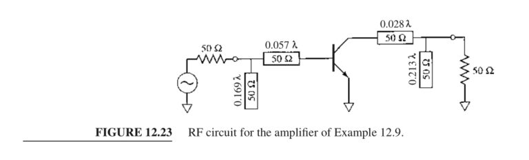
The AC amplifier circuit is shown in Figure 12.23.
For an output power of 10 W, the required input drive power is
P_{in}=P_{out}(dBm)-G(dB)=10\log (10.000)-16.4=23.6 dBm=229 mW.The DC input power can be found from the drain efficiency as P_{DC} = P_{out}/η =38.5 W, so the DC drain current is I_{D} = P_{DC}/VDS = 1.37 A. The power added efficiency of the amplifier can be found from (12.89) to be
\pmb{\eta} _{PAE}=\frac{P_{out}-P_{in}}{P_{DC}}=\frac{10.0-0.229}{38.5}=25 \%