Question 16.DA.12: A STATIC CMOS LOGIC GATE Objective: Design a static CMOS log...
A STATIC CMOS LOGIC GATE
Objective: Design a static CMOS logic gate to implement a specific logic function.
Specifications: A static CMOS logic gate is to be designed that implements the function of a three-input odd-parity checker. The output is to be high when an odd number of inputs are high. The size of each transistor is to be determined so that the switching speed is the same as that of a basic CMOS inverter with W_{n} = W and W_{p} = 2 W . A minimum number of transistors are to be used in the NMOS pull-down and PMOS pull-up portions of the circuit.
Choices: We will assume that input signals A, B, and C as well as the complements \bar{A}, \bar{B}, and \bar{C} are available.
Learn more on how we answer questions.
(Logic Function): The output of the logic gate is to be high when one
input is high or when all three inputs are high. The output is to be high, for example, when the inputs are A = 1 and B = C = 0. The output would be high, then, for A \bar{B} \bar{C} = 1. Considering the other possibilities, the logic function can be written as
F = A \bar{B} \bar{C} + \bar{A} B \bar{C} + \bar{A} \bar{B} C + ABC (16.94)
(NMOS Pull-Down): Figure 16.96(a) shows the basic NMOS pull-down portion of the logic gate derived from the logic function given in Equation (16.94).
However, we may note that the two transistors at the bottom of the first two columns have a common input of \bar{C} and the two transistors at the bottom of the last two columns have a common input of C. The two transistors with common inputs can be combined into a single transistor. The final design of the NMOS pull-down portion of the logic gate is shown in Figure 16.96(b).
In order for the NMOS portion of the circuit to be in the pull-down mode, three NMOS devices in series must be turned on. In order for this circuit to be equivalent to the NMOS in the CMOS inverter, each NMOS device must have a width of W_{n} = 3 W .
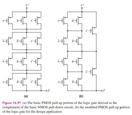
(PMOS Pull-Up): Figure 16.97(a) shows the basic PMOS pull-up
portion of the logic gate. This circuit is the complement of the NMOS circuit shown in Figure 16.96(a). We may note that two transistors on the right side of the circuit have common inputs C and \bar{C} . Each pair of transistors is effectively in series and hence can be replaced by a single transistor. The resulting circuit is shown in Figure 16.97(b). The complete three-input odd-parity checker circuit is then the combination of Figures 16.96(b) and 16.97(b) along with a CMOS inverter on the output.
Comment: The basic logic circuit can be derived from the logic function.
However, as we have seen, some simplifications can be made in the design. These simplifications can also be obtained from simplifications in the basic logic function also.