Question 16.11: Objective: Design a CMOS logic circuit to implement a partic...
Objective: Design a CMOS logic circuit to implement a particular logic function. Implement the logic function Y = AB + C(D + E) in a CMOS design. The signals A, B, C, D, and E are available.
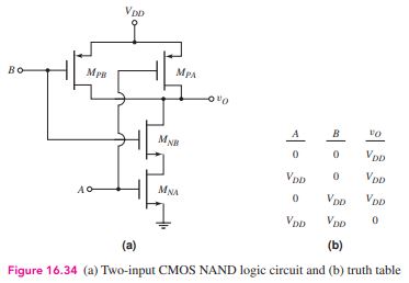
Design Approach: The general CMOS design is shown in Figure 16.38, in which the inputs are applied to both PMOS and NMOS networks. We may start the design by considering the NMOS portion of the circuit. To implement a basic OR (NOR) function, the n-channel transistors are in parallel (Figure 16.33) and to implement a basic AND (NAND) function, the n-channel transistors are in series (Figure 16.34). We will consider whether the function or its complement is generated at the end of the design.


Learn more on how we answer questions.
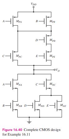
(NMOS Design): In the overall function, we note the logic OR between the functions AB and C(D + E), so that the NMOS devices used to implement AB will be in parallel with the NMOS devices used to implement C(D + E). There is a logic AND between the inputs A and B, so that the NMOS devices with these inputs will be in series. Finally, the NMOS devices with the D and E inputs will be in parallel and this combination will be in series with the NMOS device with the C input. The NMOS implementation of the function is shown in Figure 16.39.
(PMOS Design): The arrangement of the PMOS devices is complementary to that of the NMOS devices. PMOS devices that perform the basic OR function are in series and PMOS devices that perform the basic AND function are in parallel. We then see that the PMOS devices used to implement AB will be in series with the devices used to implement C(D + E). The two PMOS devices with the A and B inputs will be in parallel. The two PMOS devices with the D and E inputs will be in series and in turn will be in parallel with the PMOS device with the C input. The completed circuit is shown in Figure 16.40.
By considering various inputs, we may note that the output signal of the circuit shown in Figure 16.40 is actually the complement of the desired signal.
We may then simply add a CMOS inverter to the output to obtain the desired function.
Comment: As mentioned, there are formal ways in which to design circuits. However, in many cases, these circuits can be designed by using the knowledge and intuition gained from previous work. The width-to-length ratios of the various transistors can be determined as we have done in previous examples.